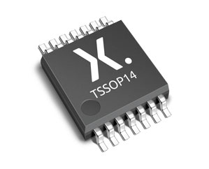

The 74AUP2G0604 is a single inverting buffer with open-drain output and a single inverter. It features two input pins (nA), an output pin (2Y) and an open-drain output pin (1Y).
Schmitt trigger action at all inputs makes the circuit tolerant of slower input rise and fall times across the entire VCC range from 0.8 V to 3.6 V.
Wide supply voltage range from 0.8 V to 3.6 V
High noise immunity
Complies with JEDEC standards:
JESD8-12 (0.8 V to 1.3 V)
JESD8-11 (0.9 V to 1.65 V)
JESD8-7 (1.2 V to 1.95 V)
JESD8-5 (1.8 V to 2.7 V)
JESD8-B (2.7 V to 3.6 V)
ESD protection:
HBM JESD22-A114F Class 3A exceeds 5000 V
MM JESD22-A115-A exceeds 200 V
CDM JESD22-C101E exceeds 1000 V
Low static power consumption; ICC = 0.9 μA (maximum)
Latch-up performance exceeds 100 mA per JESD 78 Class II
Inputs accept voltages up to 3.6 V
Low noise overshoot and undershoot < 10 % of VCC
IOFF circuitry provides partial power-down mode operation
Multiple package options
Specified from -40 °C to +85 °C and -40 °C to +125 °C
| Type number | Product status | VCC (V) | Logic switching levels | Output drive capability (mA) | tpd (ns) | fmax (MHz) | Nr of bits | Power dissipation considerations | Tamb (°C) | Rth(j-a) (K/W) | Ψth(j-top) (K/W) | Rth(j-c) (K/W) | Package name |
|---|---|---|---|---|---|---|---|---|---|---|---|---|---|
| 74AUP2G0604GM | Production | 0.8 - 3.6 | CMOS | ± 1.9 | 4.0 | 70 | 2 | ultra low | -40~125 | 290 | 6.5 | 145 | XSON6 |
| 74AUP2G0604GN | Production | 0.8 - 3.6 | CMOS | ± 1.9 | 4.0 | 70 | 2 | ultra low | -40~125 | 275 | 11.7 | 171 | XSON6 |
| 74AUP2G0604GS | Production | 0.8 - 3.6 | CMOS | ± 1.9 | 4.0 | 70 | 2 | ultra low | -40~125 | 272 | 14.8 | 177 | XSON6 |
| 74AUP2G0604GW | Production | 0.8 - 3.6 | CMOS | ± 1.9 | 4.0 | 70 | 2 | ultra low | -40~125 | 264 | 38.6 | 153 | TSSOP6 |